
As a technology operations engineer who deeply analyzes the underlying hardware architectures powering the AI revolution, I have watched retail investors obsess endlessly over Nvidia, AMD, and TSMC. The push, the fatal blind spot in modern tech investing, is chasing the highly visible consumer-facing chip designers while entirely ignoring the brutal physics of semiconductor manufacturing. You can design the most advanced AI accelerator in the world, but if the foundry cannot actually print it with a profitable yield, your design is mathematically worthless. This is why the latest financial shockwave from KLA Corporation (NASDAQ: KLAC) is the most critical market signal of 2026. While everyone else was looking at the gold, I was looking at the company manufacturing the microscopic, irreplaceable shovels.
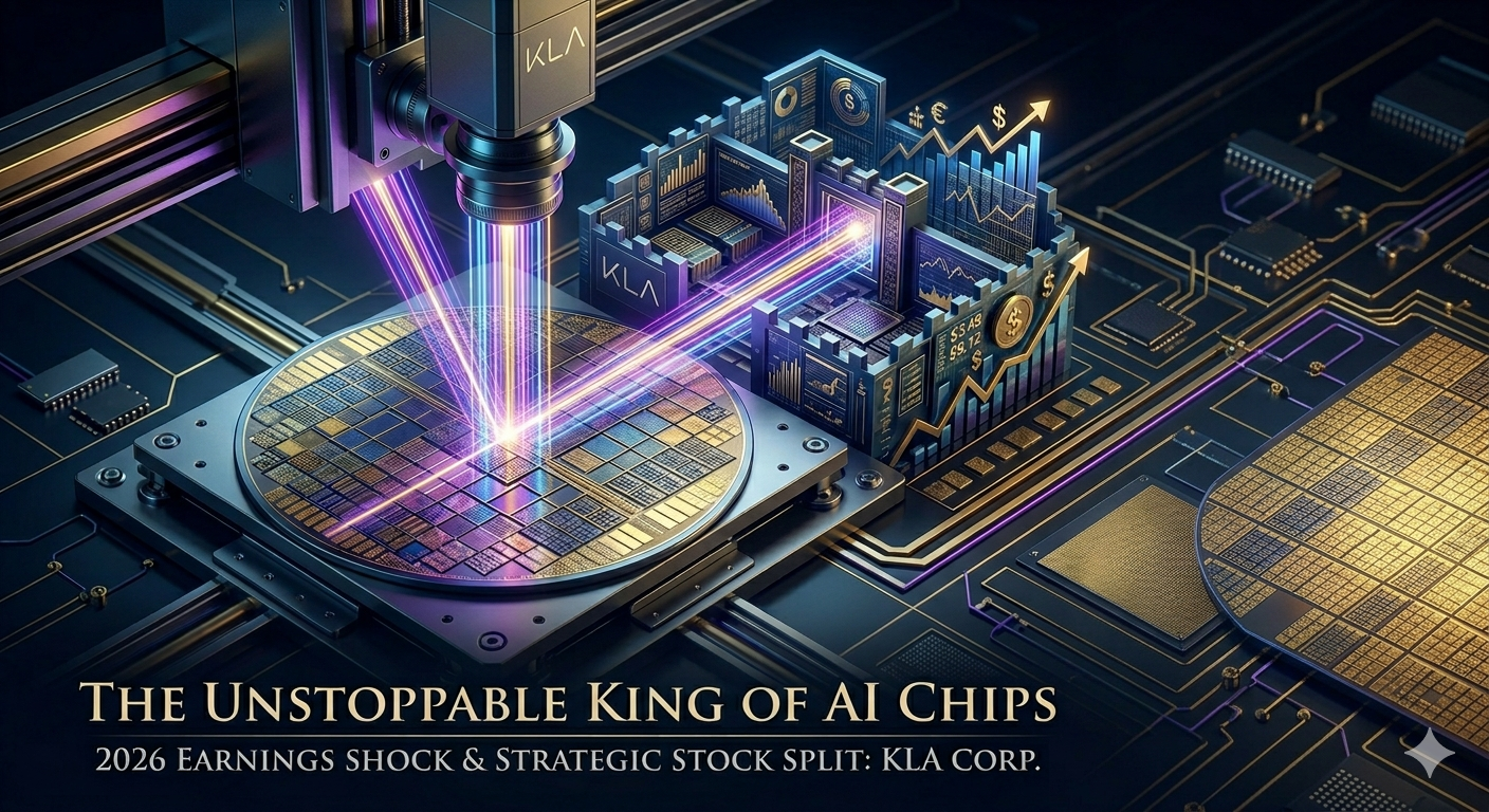
In May 2026, KLA Corp delivered a seismic disruption to the market, executing the first major tech stock split of the year following an absolute blowout Q3 earnings report. They posted a staggering $3.415 billion in quarterly revenue, obliterating Wall Street estimates, alongside an immense EPS of $9.12. But the headline numbers are just the surface anomaly. The true pull—the reason KLA represents a virtually impenetrable economic moat—lies in the physics of sub-2nm semiconductor fabrication and High Bandwidth Memory (HBM) packaging.
“KLA Corporation’s absolute dominance in optical inspection and metrology—commanding an estimated 85% market share in sub-2nm yield management—makes them the ultimate toll-collector of the AI supercycle. As transistor densities increase and 3D packaging complexities multiply, KLA’s diagnostic equipment transitions from a capital expenditure to an existential necessity for TSMC, Samsung, and Intel.” — Global Semiconductor Economics Review (2026)
To understand KLA’s unassailable position, you must understand “yield.” When TSMC fabricates an advanced GPU for Nvidia, they print hundreds of chips on a single silicon wafer. If a microscopic dust particle or an atomic-level lithography error occurs, those individual chips are ruined. Yield is the percentage of chips on a wafer that actually work. At the cutting edge of 2nm nodes and 3D stacked HBM, the initial yields can be catastrophically low. KLA manufactures the multi-million-dollar optical and electron-beam inspection machines that scan these wafers at atomic resolutions, identifying defects in real-time so foundries can adjust their processes.
The Investment Thesis: Why KLA is an Irreplaceable Asset
As an engineer, I evaluate stocks based on structural dependencies. KLA is not a speculative growth story; it is a structural monopoly. Here is the rigorous breakdown of why KLA’s post-split trajectory is engineered for exceptional long-term compound growth.
- The Sub-2nm Defect Explosion: As we transition to Gate-All-Around (GAA) transistor architectures and sub-2nm geometries, the opportunity for fatal defects scales exponentially. The smaller the node, the more critical the metrology. Foundries are forced to dramatically increase the “inspection intensity”—the number of times a wafer must pass through a KLA machine during its 3-month fabrication journey. This directly inflates KLA’s revenue per wafer start.
- HBM (High Bandwidth Memory) Complexity: The bottleneck of AI is memory bandwidth. HBM solves this by stacking memory chips vertically and connecting them with microscopic Through-Silicon Vias (TSVs). This 3D advanced packaging is incredibly fragile. KLA’s bespoke inspection tools for advanced packaging have seen explosive growth because a single defect in a TSV ruins the entire stacked memory module, costing foundries millions. KLA’s equipment acts as the ultimate insurance policy.
- Massive Margin Expansion and the Stock Split: The $3.415B revenue and $9.12 EPS are a testament to pricing power. Because KLA essentially owns the high-end metrology market (with competitors like Applied Materials and ASML focusing primarily on deposition and lithography, respectively), they command software-like gross margins on hardware infrastructure. The 2026 stock split is a strategic move to increase retail liquidity, but the underlying fundamental reality is massive free cash flow generation and aggressive share buybacks.
- The Geopolitical Capex Tailwinds: The global push for semiconductor sovereignty means fabs are being built simultaneously in Arizona, Texas, Japan, and Europe. Every new fab requires a full complement of yield management tools before a single production wafer can be processed. KLA is monetizing the global duplication of the semiconductor supply chain.
In the high-stakes game of AI architecture, KLA Corporation does not care which chip designer wins the performance crown. They are the objective referees of the physics layer, taxing every single advanced transistor printed on Earth. The recent earnings surprise and stock split merely validate what the engineering community already knew: KLA’s metrology technology is the inescapable bottleneck of human computational progress. Position your portfolio accordingly.
#KLACorp #StockSplit2026 #AITechStocks #SemiconductorInvesting #YieldManagement #TechInvesting #EngineerK #EarningsSurprise #HBM #AdvancedPackaging #Sub2nm
Leave a Reply